How Design Impacts PCB Manufacturing Process
PCB design is a complex process. Careful considerations, down to the tiniest detail, must be made. All of your design choices will affect one or more stages of the PCB manufacturing process. This includes everything from shape and size to what type of drill hole technology you use. Failing to pay attention to how your design will affect the PCB fabrication process can take weeks of work right down the drain as you go back to the drawing board for a redesign. To keep everything on track, it is important to truly understand the PCB manufacturing process from beginning to end so you make the best possible design choices right from the start.
The PCB Manufacturing Process
Understanding the PCB manufacturing process means knowing all of the steps that go into it. This is split into two phases; the PCB fabrication process and the PCB assembly. Both are equally important, and your design choice will determine the success of each phase.
PCB Fabrication Process
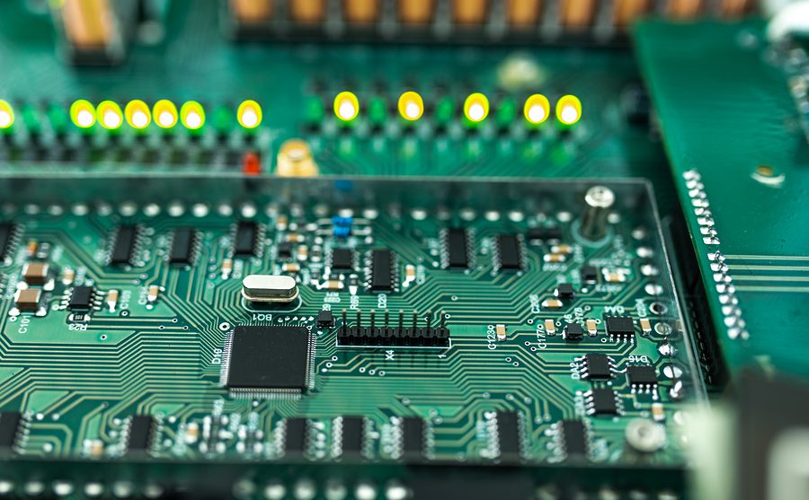
The PCB fabrication process begins with creating the board itself. It must be compatible with the PCB layout as dictated by the design. It all starts with imaging the schematics on the board with a laser.
From there, excess copper is removed from the board by etching. In the case of multilayer boards, they will be built up by heating and pressing the layers together at this point.
Next, mounting holes are drilled, followed by more copper etching. At this point your board is about halfway complete.
As board manufacturing process continues, plating begins. The panel undergoes a series of chemical baths to deposit extremely thin layers of conductive copper over the surface of the panel, including into the recently drilled holes.
Next, a thin layer of solder masking is added to the surface to separate any conductive elements and help prevent oxidation.
Once this is complete, the PCB design is silkscreened onto the board. This includes all locations of pins and other important information, like part numbers.
Finally, finishing occurs. The surface is chemically coated to protect it from oxidation and other environmental risks. Multiple types of surface finishes can be used depending on the environment and board components. Surface finish options can include gold, silver, lead, and tin.
PCB Assembly
PCB assembly begins with your bare board. The first step is to apply a solder paste to the board which prepares it for component mounting.
Assembly moves to the pick and place machine. This automated device will place surface mount components on your board.
Next, is solder reflow. The components need to stay in place, so the solder paste is heated to adhere components to the board.
Any connections that are not secure after this step will require manual re-soldering.
If your board requires through-hole technology, those components will be mounted next. Then wave soldering will be used to secure the through-hole mounted components.
Another round of final soldering will then take place after inspections uncover any components that have not securely adhered to the board.
Finally, your board is thoroughly cleaned with a solvent to remove any excess resin or other contaminants. Your board is now ready to be packed up and shipped out.
Design for Manufacturability
A design for manufacturability (DFM) analysis can do a lot to make sure your design is optimized before the PCB manufacturing process begins. A DFM performed by your ECM will determine if your design meets the requirements of the manufacturing process to actually produce a PCB. DFMs can detect design issues that could lead to manufacturing problems. You can them go back and rework your design to eliminate these potential problems early.
Correcting issues that will affect manufacturing early on allows you to do so before it’s too late. Overlooking design issues could be costly. They could shut down production and send your project back to square one for re-engineering. If that happens, it will likely cost you a lot of time and money.
If your design is ready to move onto the PCB manufacturing process, consider choosing Levison Enterprises as your electronic contract manufacturer. We take customer satisfaction seriously, so you can be sure our team will always be available to assist you with any aspect of your design. Think of us as an extension of your own team. Contact us today for information on our DFM analysis services and see how we can turn your design into a dynamite product.