Guide to Understanding the PCBA Electronic Manufacturing Process
The world of electronics and electronic manufacturing is constantly changing. It’s an industry with a rapid pace evolution and shows no signs of slowing down, but the printed circuit board assembly (PCBA) process is one standard among this swift progression.
A project manager needs an electronic contract manufacturer or ECM he/she can depend on for a steady and proven PCBA process that can handle advancements in electronics and the PCB components that control them. Before finding the ECM partner to tackle your project you should truly understand how your printed circuit board is made from quote to prototype to finished product. Here is your guide to understanding the PCBA process.
Quote Phase
Believe it or not, the quote phase can be the most important factor for your PCBA project’s success. The quote you receive from your ECM spells out the time requirements, cost, and details of what you can expect in the completed product. Your ECM will look over your PCB design for inaccuracies and obsolete parts. Based on your design, assembly requirements, bill of materials, and other basic project information you provide, your ECM will provide you with a design for manufacturability (DFM) analysis. The DFM analysis from your ECM can assist in a re-engineer and/or design in order to reduce manufacturing costs of you PCBs by saving both time and money. The aim here is to fix potential problems, and the design phase is the least expensive place to address them.
Prototype Phase
The project manager takes over during the prototype phase. This is a crucial stage to your project’s development. It ensures your design works perfect before a full run of your printed circuit boards is made. The prototype allows your ECM to make sure all parts are in house before production begins and for you to test your PCB’s functionality. The prototype also helps save money by eliminating failures early. It avoids the cost of a whole production run of faulty boards by detecting flaws in the production process. Once you’re satisfied with your prototype, your project is nearly ready for a full production run.
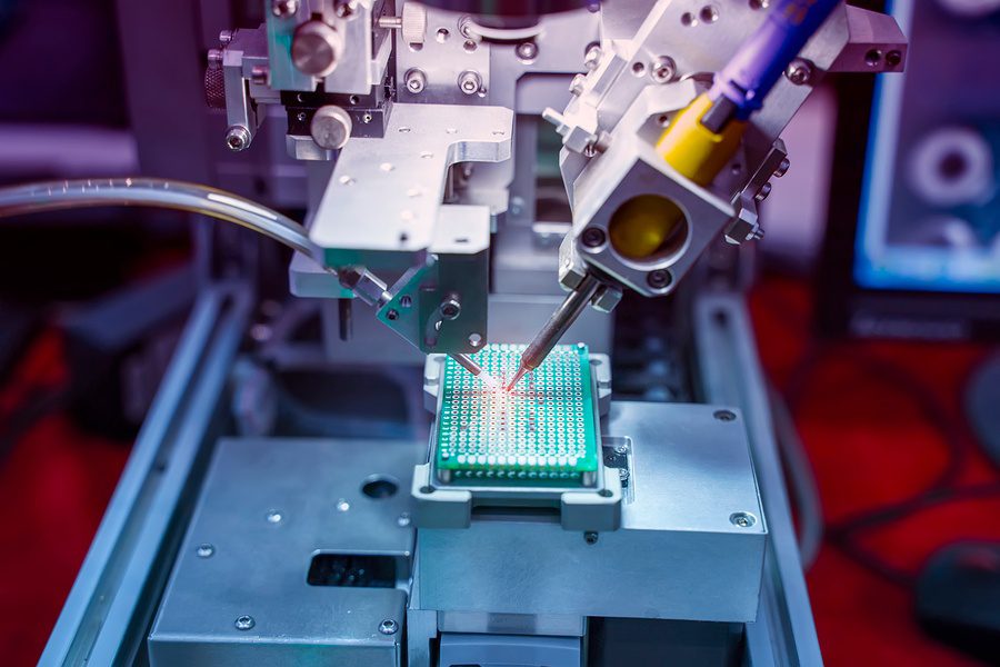
Solder Phase
There are two types of assemblies used in the solder phase of your PCB assembly; pick and place surface mount technology (SMT) and through-hole technology (THT).
Pick and Place
Surface-mount technology (SMT) is a newer method for producing electronic circuits in which the components are mounted or placed directly onto the surface of printed circuit boards (PCBs). A robotic device called a pick and place machine places surface mount components or devices (SMDs) on a prepared PCB. The SMDs are then soldered on to the surface of the board. Most non-connector components on modern PCBs are SMDs.
Through-Hole Technology
Through-hole technology refers to the mounting method used for electronic components that involve the use of leads on the components that are inserted into holes drilled in printed circuit boards and soldered to pads on the opposite side. This is done by either manual assembly or by the use of a wave-soldering machine. Every component on a circuit board was a through-hole component from the 1950s until the mid-80s when SMT became popular.
Both technologies can be used on the same board. Through-hole technology will be used for components not suitable for surface mounting such as large transformers and heat-synced power semiconductors.
Inspection
Once components are soldered in place, your PCBs will move on to inspection. Checking for errors and misalignments can ensure that errors are found and fixed as soon as possible. This helps both the manufacturer and the designer save time, labor, and materials. Perhaps the most comprehensive inspection methods of modern circuit boards is automatic optical inspection (AOI). It is nearly impossible for smaller and more complicated circuits manufactured today to be manually inspected in order to detect internal defects. An AOI machine uses a series of high-powered, autonomous cameras to scan devices for missing components or quality problems and to examine the quality of solder connections. The AOI does this at a very high speed, allowing it to process a high quantity of PCBs in a relatively short time.
Testing
The next step of the process, if desired by the customer, is to test your printed circuit board to make sure it does what it’s supposed to do. This involves testing the PCB connections for quality and putting it through its paces using testing fixtures. It will be checked to see how it functions under normal conditions in which it will operate. If desired, a PCB must pass the testing phase in order to be considered complete and shipped to you for use in your final product.
Email SalesWhy Chose Levison?
You want, need, and deserve a PCB assembly partner committed to you and your product. Levison Enterprises demonstrates a commitment to high quality for your electronics manufacturing needs. We strive to deliver products and services that not only meet but exceed your expectations. Levison Enterprises is an ISO 9001 certified electronics manufacturer, committed to delivering you a rigorously tested, high quality product. We also maintain IPC and J Standard Certification and ITAR registration for your defense-related materials and projects. Start your PCBA process today by contacting us for a free quote.