6 Tips For Electronic Manufacturing PCB Design
It is sometimes said that PCB design is 90% placement and 10% routing. That may be the case, but both beginners and experienced designers can get caught off guard by simple oversight. It doesn’t take much to turn a successful design of a printed circuit board into a high-tech disaster. It is best to know what to watch out for in order to avoid potential problems. Here are some tips from professional electronic manufacturers to help you avoid function and reliability problems in your PCB design.
1. Hardware
Before you even start to plan your PCB assembly, you need to make sure you’re set up to start designing. You will want a powerful computer with as much speed and memory as you can get to run your CAD system. You can stick with a mouse and keyboard you are most comfortable with, but you will want a larger monitor. The bigger the monitor is, the easier it will be to see details while designing elaborate schematics. You may also want to consider multiple monitors to keep you organized.
2. Know the Production Process
You must know how a PCB is produced if you are going to design one. Learn everything you can about the prototype and manufacturing processes. Your ECM will be a wealth of knowledge, so talk to them and ask questions. Understanding how a PCB is made will help you develop a better design. Sometimes PCBs have overly complicated designs that are difficult, or even impossible to complete. Complex designs can stall the prototype process and call for re-engineering. This can waste time and increase costs.
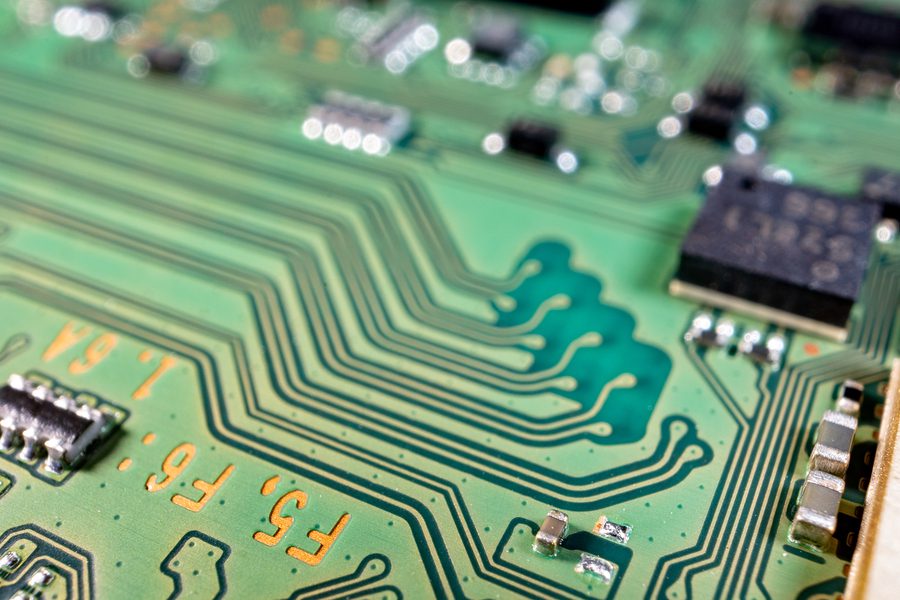
3. Use Your Autorouter Sparingly
Autorouters are common tools in PCB design software, however, it is best to create your own routing traces. Autorouter tools are not always accurate and can cause you major headaches. Doing it yourself will also enable you to create a more symmetrical design.
Once you have placed your components, you may consider using an autorouter to check your work. The tool can check your completion rating to see if you need to make adjustments. It can also help you discover bottlenecks and other problems with connection points.
4. Don’t Skip the Schematic
Schematics are extremely important for ensuring your PCB design will be successful. You need to be able to organize elements near their practical components. A schematic makes this possible by giving you a way to visualize the circuit. Without it, you might miss a disconnection or even skip over obvious engineering flaws.
5. Leave Room Between Traces and Mounting Holes
Not leaving enough room between traces and mounting holes is a common mistake in PCB design and results in a shock hazard on your board. It is best to leave a ring of space beyond the physical dimensions of the mounting hole. This will protect it from nearby components and traces.
6. Watch for Slivers
Beware of hidden elements that can diminish your circuit board’s functionality. The most common problems are solder mask or copper wedges that develop during the etching process. These are called slivers. They can also appear if part of the PCB design is too slim or too deep. A simple DFM check can predict your potential for slivers, however, they are most easily avoided by following the minimum width standards.
Knowledge is power, and following these simple tips can help you attain PCB design success. Remember to take your time and seek help if you need it. The designers and engineers at Levison Enterprises can help if you get stuck. Levison Enterprises team of experienced engineers can also give you a second set of eyes on your design before you begin the prototype process. We want your project to be a success. Contact Levison Enterprises today to find out how we can help make that happen.